
1. Describe The Concept of Holes.
Answer: Concept of Holes:
We know, Due to thermal agitation, the covalent band breaks down, the electron in covalent band gain energy to jump into conduction band leaving an positively charged "Empty Space" in valence band.
The movement of valence electron into the empty space in equivalent to the movement of the positively charged empty state itself

it's shown the valence electron band a movement to fill the empty space.
So the crystal now has a second equally change carrier that can contribute in current flow this charge carrier is called hole .2. Discuss Density of Allowed Energy State as Function of Energy with Necessary sketch.
Answer: In order to calculate the electron and hole concentrations the density of allowed energy states as a function of energy is need to determine.
The density of quantum state as a function of energy(E) is given bellow for a free electron

Now for semiconductor, this will become

This equation will be valid if E>Ec.
So if the energy of the electron in the conduction band decrees the number of available quantum states decreases for valiance band,


3. Discuss Statistical Distribution of Materials.
Answer:

4. Derive the equations for the thermal equilibrium contractions of electrons and holes in term of Fermi level.
Answer: The equation at of concentration of electron at thermal equilibrium may be
find by
the lower limit of integration is Ec and upper limit of integration should be the allowed conduction band. As fE(E) is rapidly approaches zero with increasing energy; So we can take the upper limit of integration to be infinity, for electrons in the conduction band , if (Ec - Ef) >>KT ; then (E-Ef)>>KT. So that the fermi probability function reduces to the Boltzmann approximation

Applying the Boltzmann,
The thermal equilibrium density of electrons in the conduction band is fond from.
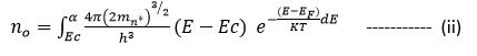

So that the thermal equilibrium electron concentration in the conduction band can be written as,

The parameter Nc is called the effective density of states function in the conduction band .
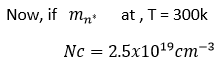 is the order of magnitude of Nc for most semiconductor.
 If the effective mass of the electron is larger smaller than m0 , then the value of Nc will Changes Accordingly.
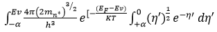
For Hole concentration: The thermal equilibrium concentration of holes in the valence band.

then, EF-Ev >>KT


Where the lower limit of integration is taken as minus infinity instead of the bottom of the valence band Let,

Now From (ii)


5. Discuss the position of Fermi level for intrinsic semiconductor.
Answer: The position of Fermi level for intrinsic semiconductor :
As we discussed earlier , the fermi level is located near the center to the forbidden band gap for state intrinsic semiconductor. Now since the electron and hole concentration are equal .
So we can write,

taking log of both side and slave for the fermi level.

again we can write


0 Comments